What does this research involve?
This theme aims to design and optimize devices used in microelectronics, with the integration of technologies towards the nanometric scale.
There are two approaches to this at ISEN Yncréa Méditerranée:
- miniaturization through a top-down approach, specific to technologies used in the microelectronics industry, with the study and design of innovative, more robust circuits;
- the study of a bottom-up approach using the incorporation of organic molecules as self-assembling building blocks on surfaces for new functionalities; this constitutes so-called molecular electronics.
How is R&D carried out?
The theme is covered by two complementary approaches: one going from the macro-system to the implementation details (top-down approach), the other starting from the basic bricks to make the system more complex and richer (bottom-up approach).
Top-Down Approach
The very low power design brings all its added value with the multitude of components, systems, products that currently flood the market. These products have the particularity to have an extremely low consumption.
One of our first activities is to provide doctoral supervision in relation to our research themes, which include reducing consumption and energy harvesting. Three thesis topics have been completed in this context in recent years:
- the one led by Maxime Cholvy, who was working on circuit design and the development of low-power analog solutions for energy management in nano power mode (nano Watt technology) for a microcontroller;
- the one led by Elie Courdouan, who was working on the development of specific multi-source energy recovery battery (BMS) modules;
- the one carried by Manon Fourniol who was working on developing a very low power measurement system (ULP) for real time environmental monitoring based on sensors (GPS, T, P, RH, RCO2, UV).
Thus, the first axis of research is the recovery of all the energies that are stored continuously (capacities, inductance). Indeed, on integrated circuits, a large number of intrinsic capacities are embedded within the circuits. The current study is to recover the charges available at time T on these capacitors during very low power modes.
This subject has been developed for several years by STMicroelectronics, and in particular in the framework of the thesis defended by Maxime Cholvy.
In parallel to this study on integrated circuit, a study was also carried out thanks to the thesis of Elie Courdouan. The objective of this thesis was to realize an intelligent system entirely autonomous in energy.
Indeed, the IoT type circuits, operating on LORA network, require little power to function. However, solar energy is already known to meet this demand for low power consumption, thanks in particular to the development of small high efficiency (and for some flexible) solar panels.
Another research axis is to quantify the vibratory energy resulting from a piezoelectric component. The conjunction of these two energy sources is then managed thanks to an intelligent Battery Management System (BMS) embedding AI, which makes it possible to meet this constraint.
Finally, a last study is to realize a very low power system (ULP), embedded on humans for medical purposes. The sensors must consume as little as possible thanks to the use of dedicated microcontroller operating modes.
This work was carried out by Manon Fourniol in collaboration with medical rehabilitation laboratories.
ISEN's Electrical Reliability Laboratory (REER) worked in the nano 2017 and RESIST projects (completed in January 2018) to strengthen ST Microelectronics as a leader in advanced technology manufacturing with the optimization of different processes (M40, 28LP, 28FD), by using accelerated lifetime techniques for MOSFET transistors and digital cells in the 40nm to 22nm gate length range.
The objective was to achieve a difficult trade-off between speed performance, power consumption and AC-DC progressive aging with increasing temperature, for multi-core and IO devices.
Emphasis was put on the comparison of RTO annealing conditions on lifetime, as well as on possible techniques to neutralize HC and temperature degradation under negative bias NBTI with hot carrier injection conditions. Different stress and recovery modes have been analyzed with direct mode substrate voltage (FBB) by sense effect of defects. This is based on the adjustment of the post-stress VT threshold voltage as a function of the number of defects and the recovery time. This has allowed the development of a methodology validated on prototype nanometer CMOS circuits (28FD) that incorporate this self-adaptive technique dedicated to automotive applications under high stress environment (T,V).
We took part in the development and testing of the first prototype digital circuits in 40LP and 28FD technologies, which adapt in real time to the trade-off between speed (frequency performance), power consumption (LP) and aging. Various variability factors (PVT) impact circuit performance:
- high temperature aging under negative bias (NBT);
- hot carrier injection (HCD);
- breakdown of the gate dielectrics (SBD, HBD).
All of these mechanisms result in a progressive temporal variability that increases the rate of error occurrence at the circuit and system level.
Error density profiles as a function of activity rate and workload were studied first through static compensation techniques (S-AVS) and then using dynamic compensation (D-ABB).
The incorporation of in-situ monitors, temperature sensors, and error correction blocks allowed for real-time adaptation of the trade-off in frequency, power consumption, and error rate variation/correction with aging for different uses.
Long term tests on boards have allowed to refine the selection of the best compensations of the D-ABB reliability by integrating the aspects of monitors, process variability, software suite, and by extending to the fine use of statistical learning algorithms with short and long term memory management leading to the development of demonstrators.
This internationally acclaimed work rewarded the efforts of PhD student Souhir Mhira (Best paper ITC 2017, Outstanding and Best paper IRPS 2017, invited paper ESREF 2018). They also allowed the validation of the first automotive FDSOI (28FD) products from ST Microelectronics for a real-time self-adaptive optimization of digital circuits dedicated to high stress applications.
In 2019, we started a study on the reliability of high voltage (HV) and low voltage (LV) technologies for imagers that are based on BiCMOS and CMOS technology, in the IPCEI project with ST Microelectronics Crolles, as a continuation over the next four years of the nano project (nano 2022).
The objective is the determination of the lifetime of these devices and circuits dedicated to the diversification of the applications stemming from the use of BiCMOS and CMOS circuitry under high activity stresses at high temperature.
The aspects of variability and impact of high temperature are therefore paramount with specific tests for the digital and analog domain. The project is developed by Alain Bravaix at ISEN Toulon since 2019 through the nano 2022 project. At the same time, another PhD student is developing a thesis at ST Rousset on the effects of local and global variability for C40 technologies (digital and memory application) through a CIFRE contract in collaboration with ISEN-Toulon.
Bottom-Up Approach
In molecular electronics, the achievements concern :
- nanostructuring of surfaces by a non-lithographic approach allowing to reach sizes not accessible by lithography;
- the study of structure-property relationships;
- self-assembly of donor-acceptor molecular systems that can lead to organic solar cells;
- the realization of self-assembled molecular nanodiamonds on the next generation of faster germanium-based transistors.
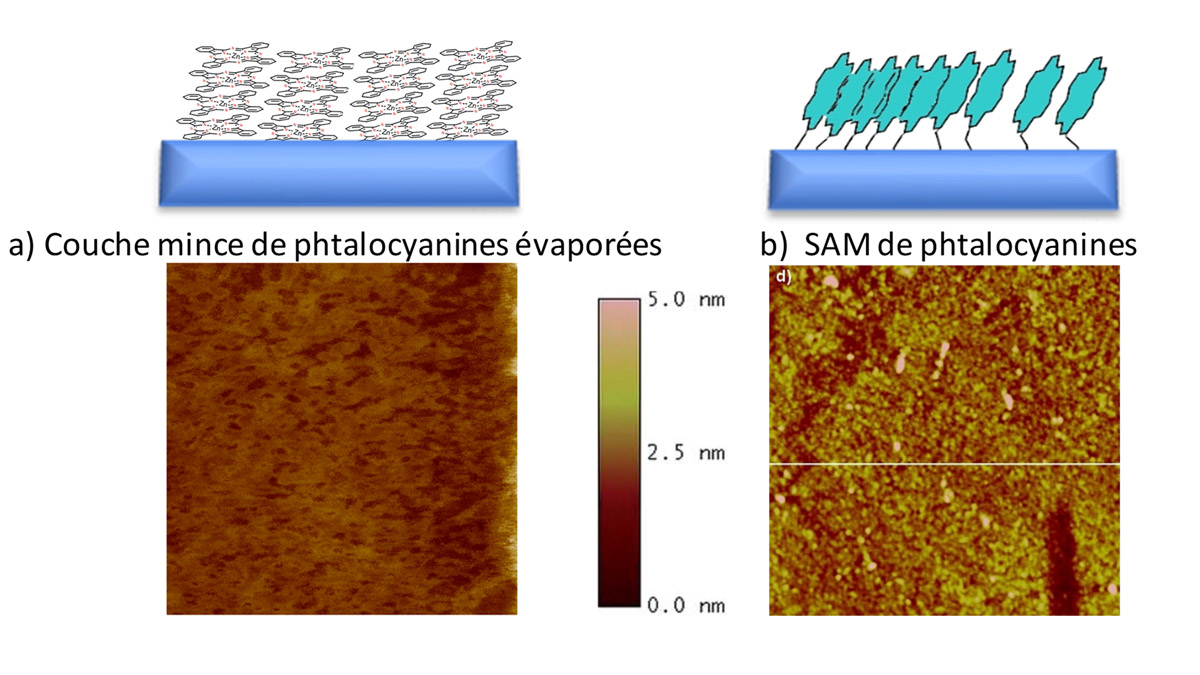
Molecular electronics is one of the promising avenues of nanoelectronics based on the use of the monolayer self-assembly potential of organic molecules and their chemically scalable electronic properties.
It is in this perspective that the work carried out at ISEN Yncréa Méditerranée within the team "Nanostructuration" of IM2NP UMR CNRS 7334 is placed. From 2002 to 2006, our work focused on molecular nanostructuring on the surface of silicon to serve as a basis for the realization of hybrid molecular nano-components compatible with silicon technology. The studied molecules were trichlorosilane-terminated molecules, deposited by self-assembly from a solution comprising one or two molecular species to obtain nanostructures by phase separation (thesis of S. Desbief, University of Provence - Aix-Marseille, defended in 2006).
Within the framework of two projects, our work was then directed more specifically towards memory cells, with the realization of a CMOS compatible memory cell where our contribution concerned a fundamental study of the role played by the molecule-electrode link (ANR PNANO "MEMO", 2005-2009), and innovative organic memories (European project "EMMA", 2006-2009) with the study and characterization of organic memory cells by near field microscopy.
Continued research activities focused on three new topics associated with three doctoral theses dedicated to the self-assembly on various surfaces (silicon, gold, etc.) of specific molecules such as conjugated macro-cycles (thesis of V. Gadenne, Univ. Aix-Marseille III started in 2006 and defended in 2010), C60 fullerenes (thesis of G. Delafosse, started in 2007 and defended in 2011), and push-pull molecules for photovoltaics with the theses of V. Malytskyi (Aix-Marseille Univ. AMU, 2011-2014), in collaboration with CINaM UMR CNRS 7325.
All these molecules have a strong potential of applications within components, in particular for memory cells and for organic photovoltaics with a wide spectral absorption range modulated by the choice of donor or acceptor groups.
Electronics and photovoltaics are still at the heart of our current research activities. In the field of photovoltaics we can mention, in addition to the thesis of V. Malytskyi, the financing by the Fonds France Canada pour la Recherche of a collaboration and of the thesis of Y. Dufil (AMU-Queen's Univ. cotutelle, 2013-18) in cotutelle with the group of Prof. J.M. Nunzi at Queen's Univ. in Canada on molecular layers and nanoparticles for photovoltaics.
And, for electronics, the ANR project "SAGe III-V" (2011-2014) with CEA, IEMN, and CINaM, concerning the design and evaluation of high permittivity molecular nanodielectrics on germanium and III-V semiconductors, which are envisaged to constitute the next generation of high frequency transistors. These nanodielectrics can be realized with push-pull molecules due to their electric dipole. This last subject is the subject of a thesis.


